歡迎光臨~泰州巨納新能源有限公司
語(yǔ)言選擇:
 ∷
∷

∷
 ∷
∷
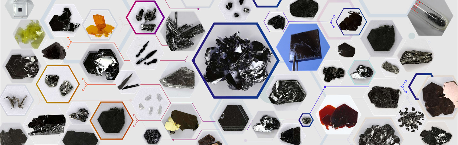


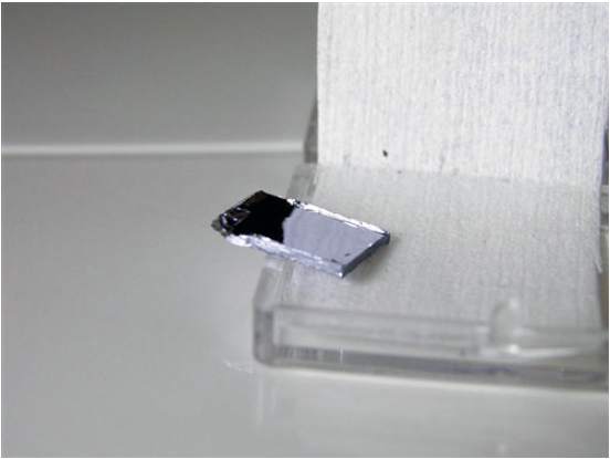
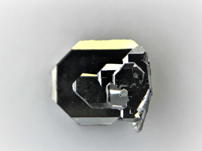
ZrSiS as a theoretically predicted and experimentally proven Dirac semimetal, exhibiting Fermi liquid behavior with two Fermi pockets at low temperatures. It sustains Weyl fermions when magnetic field is applied. It has been also shown that it may evolve to a topological insulator under the external stimuli. ZrSiS crystallizes in tetragonal phase (space group P4/nmm) with lattice parameters of a=b=3.545?? and c=8.05??. The crystal structure of ZrSiS can be described as a typical layered compound of quintuple layers of S-Zr-Si-Zr-S. Each order contains 2-3 pieces of few mm sized (2-3mm) crystals that are perfectly oriented in their basal plane for easy and efficient exfoliation process, STM / ARPES characterization, and electronic measurements.
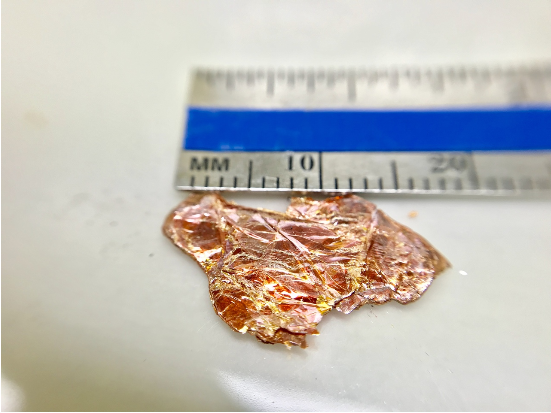
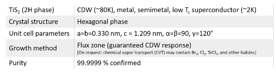
Material properties of ZrSiS crystals: Dirac semimetal, Weyl fermion, and topological insulator
Growth method matters> Flux zone or CVT growth method? Contamination of halides and the presence point defects in layered crystals are well known cause for their weak CDW response, high electronic resistivity, and environmental instability. Flux zone technique is a halide free and slow growth technique used for synthesizing high-quality vdW crystals. This method distinguishes itself from chemical vapor transport (CVT) technique used by others in the following regard: CVT is a quick (~2 weeks) growth method but exhibits poor crystalline quality and the defect concentration reaches to 1E11 to 1E12 cm-2 range. In contrast, flux method takes long (~3 months) growth time, but ensures slow crystallization for perfect atomic structuring, and impurity free crystal growth with defect concentration as low as 1E9 - 1E10 cm-2.
During check out just state which type of growth process is preferred (CVT vs Flux zone). We recommend flux zone, and unless otherwise stated, 2Dsemiconductors ships Flux zone crystals as a default choice.
聯(lián)系人:嚴(yán)春偉
手機(jī):13914543285
電話:0523-86190619,86192878
郵箱:taizhou@sunano.com.cn
地址: 江蘇省泰州市鳳凰西路168號(hào)