歡迎光臨~泰州巨納新能源有限公司
語言選擇:
 ∷
∷

∷
 ∷
∷

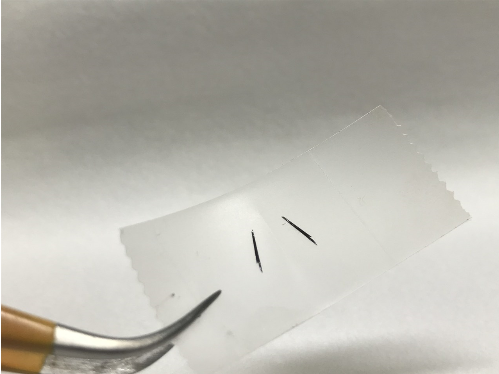
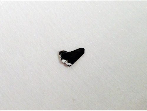
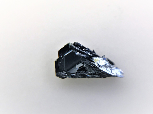
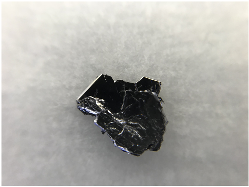
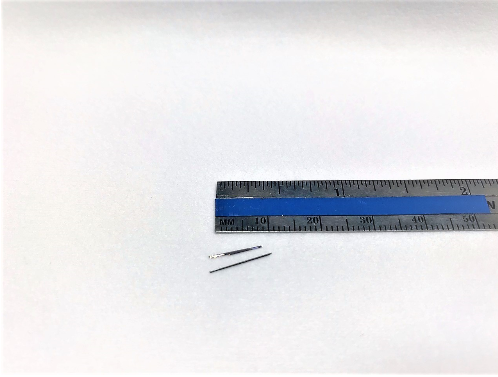
Zirconium triselenide belongs to the group-IV transition metal trichalcogenides. This is the only commercially available ZrSe3 crystals in the market, and our crystals have been engineered to attain rather low record defect density (1E9-1E10cm-2) to yield environmentally stable ZrSe3 crystals. ZrSe3 crystals exhibit semimetallic behavior with charge density waves (CDW) phenomena and even possess a superconducting response at low temperatures. ZrSe3 behaves semiconducting as well as metallic depending on the physical thickness of the material, and exhibit CDWs. Recent studies have proposed ZrSe3 as fermoelectric [1], high carrier mobility 2D transistors [2], new IR material [3-4], as well as polarized emission material [4]. In a typical order, a large number of layered needle like sheets are contained in a capsule sealed under Argon environment. The layers are stacked together via van der Waals interactions and can be exfoliated into thin 2D layers.
Growth method matters> Flux zone or CVT growth method? Contamination of halides and point defects in layered crystals are well known cause for their reduced electronic mobility, reduced anisotropic response, poor e-h recombination, low-PL emission, and lower optical absorption. Flux zone technique is a halide free technique used for synthesizing truly semiconductor grade vdW crystals. This method distinguishes itself from chemical vapor transport (CVT) technique in the following regard: CVT is a quick (~2 weeks) growth method but exhibits poor crystalline quality and the defect concentration reaches to 1E11 to 1E12 cm-2 range. In contrast, flux method takes long (~3 months) growth time, but ensures slow crystallization for perfect atomic structuring, and impurity free crystal growth with defect concentration as low as 1E9 - 1E10 cm-2. During check out just state which type of growth process is preferred. Unless otherwise stated, 2Dsemiconductors ships Flux zone crystals as a default choice.
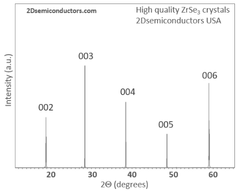
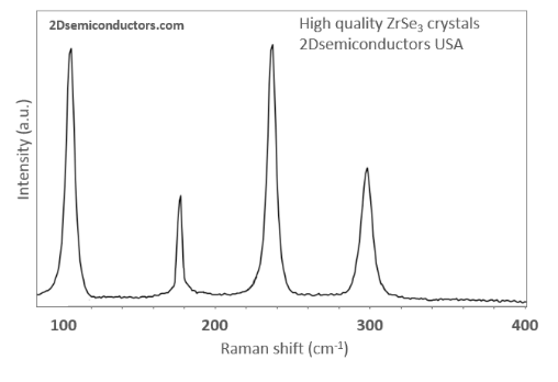
Properties of CDW ZrSe3 crystals
Related literature
[1] "ZrSe3-Type Variant of TiS3: Structure and Thermoelectric Properties"; Chem. Mater., 2014, 26 (19), pp 5585–5591
[2] "Titanium Trisulfide Monolayer: Theoretical Prediction of a New Direct-Gap Semiconductor with High and Anisotropic Carrier Mobility"; Angew Chem Int Ed Engl. 2015 Jun 22;54(26):7572-6 [Link]
[3] Single layer of MX3 (M = Ti, Zr; X = S, Se, Te): A new platform for nano-electronics and optics; Phys.Chem.Chem.Phys.,2015, 17, 18665
[4] Angle resolved vibrational properties of anisotropic transition metal trichalcogenide nanosheets; Nanoscale, 2017,9, 4175-4182


聯系人:嚴春偉
手機:13914543285
電話:0523-86190619,86192878
郵箱:taizhou@sunano.com.cn
地址: 江蘇省泰州市鳳凰西路168號